The latest Silicon Chip has an interesting article on horribly unsafe electrical devices from overseas, you can read some of it here. Also covered are things like suicide showerheads and stuff like this.
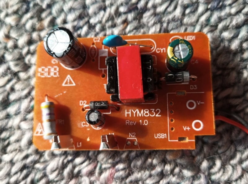
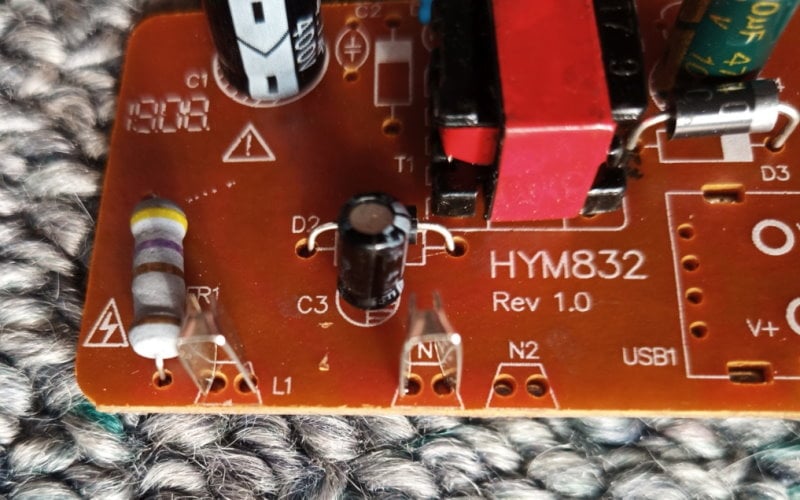
Speaking of crappy Chinese stuff, here's the 12V power supply that my ethernet optocoupler came with (fibre-optic link to remove the direct connection from stuff outside to inside the house). They came in a tiny wall wart which I'd thrown out but then pulled back out of the bin to see what was inside, the contents are as follows:
The two metal pins at the bottom are are where the prongs from the mains connector touch the PCB:
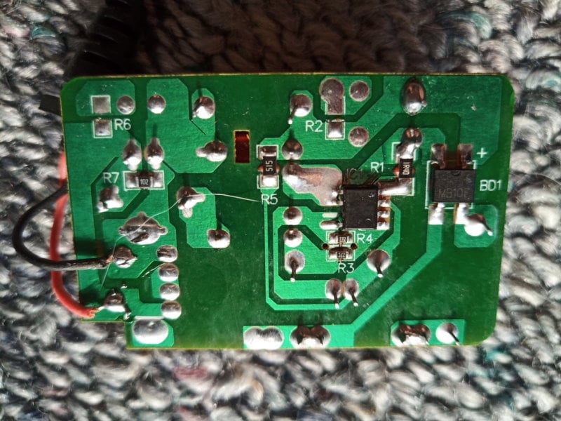
This is the underside:
Bottom right is the mains input, they've at least allowed some creepage distance before it goes into the full-wave bridge (a Diodes Inc MB10F clone), but there's no input filtering, nothing. The switchmode controller IC is totally anonymous, could be anything. And this:
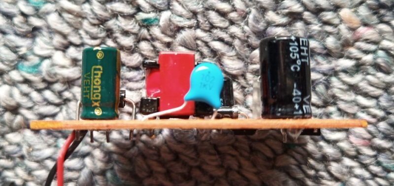
sure isn't an X/Y-rated cap.
Looks like it's a one-size-fits-all circuit since they're also using it for USB chargers and who knows what else.
Are you subscribed to our RSS feed? You can download the latest headlines and summaries from our stories directly
to your computer or smartphone by using a feed reader.